Group B
Q.no 11
D-Type Flip-Flop
A D flip-flop is widely used as the basic building block of random access memory (RAM) and registers.
A D flip flop has a single data input. This type of flip flop is obtained from the SR flip flop by connecting the R input through an inverter, and the S input is connected directly to data input. The modified clocked SR flip-flop is known as D-flip-flop and is shown below. From the truth table of SR flip-flop we see that the output of the SR flip-flop is in unpredictable state when the inputs are same and high. In many practical applications, these input conditions are not required. These input conditions can be avoided by making them complement of each other.

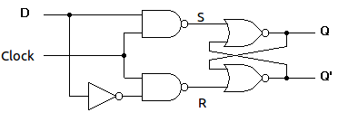
Figure-3:Circuit diagram of D flip flop
Characteristic Equation:
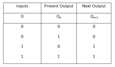
Qn+1 =DQn‘ +DQn =D(Qn‘ + Qn)
Qn+1 =D
Exicitation Table:

Q.No 12


Q.no 13


Q.No 14
This two 2 to 4 decoders can be connected in following way to use it as 3 to 8 decoder. Lower decoder will be enabled by making A2=0A2=0 and upper by making A2=1.
Q.no 15
4×1 Multiplexer
4×1 Multiplexer has four data inputs I3, I2, I1 & I0, two selection lines s1 & s0 and one output Y. The block diagram of 4×1 Multiplexer is shown in the following figure.
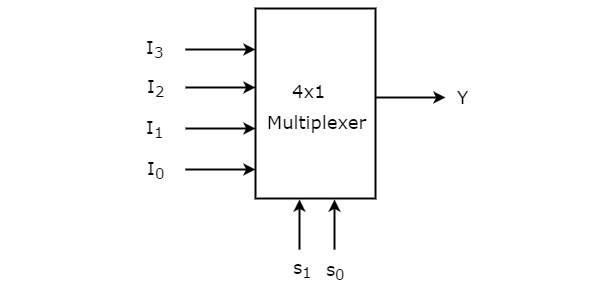
One of these 4 inputs will be connected to the output based on the combination of inputs present at these two selection lines. Truth table of 4×1 Multiplexer is shown below.
| Selection Lines | Output | |
|---|---|---|
| S1 | S0 | Y |
| 0 | 0 | I0 |
| 0 | 1 | I1 |
| 1 | 0 | I2 |
| 1 | 1 | I3 |
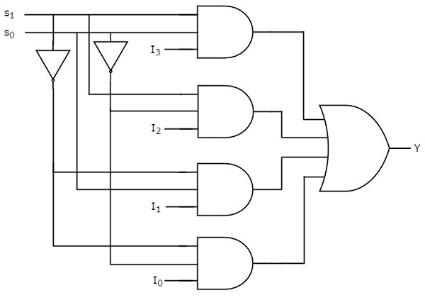
From Truth table, we can directly write the Boolean function for output, Y as
We can implement this Boolean function using Inverters, AND gates & OR gate. The circuit diagram of 4×1 multiplexer is shown in the following figure.
Group C
Q.no 16

Q.no 17


